What is 4 layer aluminum PCB? Let’s discover definition, benefits, applications, design spec and guideline, production process for 4L PCB together.
Are you troubled with these issues?
- How does a 4-layer aluminum PCB eliminate thermal overload concerns in high-power LED/power modules?
- How to achieve the perfect balance of high performance and low cost with aluminum substrates?
- How to ensure rapid yet reliable prototyping and mass production with 4-layer aluminum PCBs?
As a 4 layer PCB manufacturer, Best Technology can provide you services and solutions:
- Thermal Breakthrough: 20 years of aluminum process expertise + micro-via thermal conduction patent, boosting thermal dissipation efficiency by 30%, solving FR4 thermal buildup issues.
- Cost Breakthrough: Bulk procurement + intelligent production scheduling, reducing per-board costs by 15-20%, delivering unbeatable value in competitive markets.
- Delivery Breakthrough: 24-hour rapid prototyping + 99.2% on-time delivery, turning time into tangible value.
Welcome to contact us if you have any request for 4 layer aluminum PCB: sales@bestpcbs.com.
What Does a 4 Layer Aluminum PCB Mean?
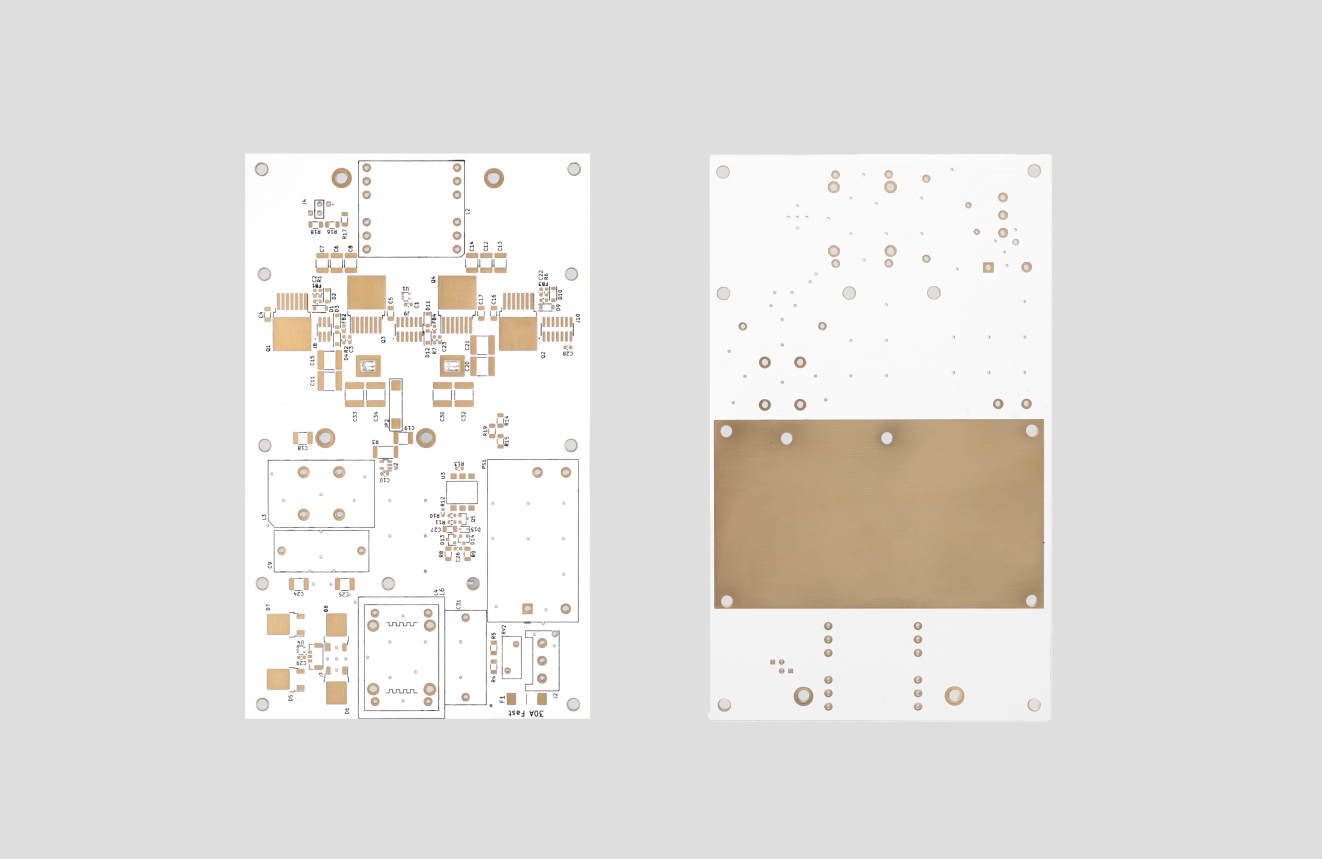
A 4 layer aluminum PCB is a printed circuit board composed of an aluminum alloy (such as 6061/5052) as the base material, forming a composite structure of “aluminum substrate layer – insulating and thermally conductive layer – multi-layer copper foil layers”.
Its core structure typically includes a 1.5-2.0mm thick aluminum substrate layer (providing mechanical support and efficient heat dissipation), a 30-100μm thick alumina-filled epoxy resin insulating layer (thermal conductivity 1.5-8 W/m·K, combining electrical insulation and thermal conduction functions), and multi-layer copper foil layers (such as 2oz copper thickness heat dissipation layer, 1oz copper thickness signal/power layer).
Why Choose 4-Layers Aluminum PCB Board?
Advantages of 4 layer aluminum PCB board:
- Enhanced Heat Dissipation & Lifespan: High thermal conductivity (1-8W/m·K) with 4-layer structure reduces thermal resistance by over 50%, minimizing overheating risks for high-heat components like LEDs/power modules, extending product life by 30-50% and cutting maintenance costs.
- Lightweight & Cost-Efficient: Aluminum is 1/3 the density of copper; 4-layer boards are 40-60% lighter than copper alternatives, with 1.0-1.6mm thickness maintaining strength. Lowers shipping costs by 20-35%, ideal for weight-sensitive applications like drones/automotive electronics.
- Improved Reliability: Matched thermal expansion coefficient (CTE) with chips reduces solder joint cracking by 40%+ via fiber-reinforced layers, lowering failure rates and boosting end-user satisfaction.
- EMI Shielding & Stability: Natural EMI shielding plus 4-layer ground plane design creates a Faraday cage effect (60-80dB shielding), minimizing signal interference and system errors, reducing debugging costs.
- Cost & Eco-Friendly Benefits: Aluminum costs 1/3 of copper; optimized trace density cuts material use, supporting SMT automation. 20-30% lower BOM costs with 15% higher production efficiency. 100% recyclable, lead/halogen-free process meets RoHS, enhancing ESG compliance.
- Robust Mechanical Performance: 250MPa+ bending strength with fiber reinforcement handles -40°C~150°C temperatures and high-vibration environments (e.g., industrial controls), reducing physical damage risks.
When to Use 4 Layer Aluminum PCB?
Applications of 4 Layer aluminum PCBs:
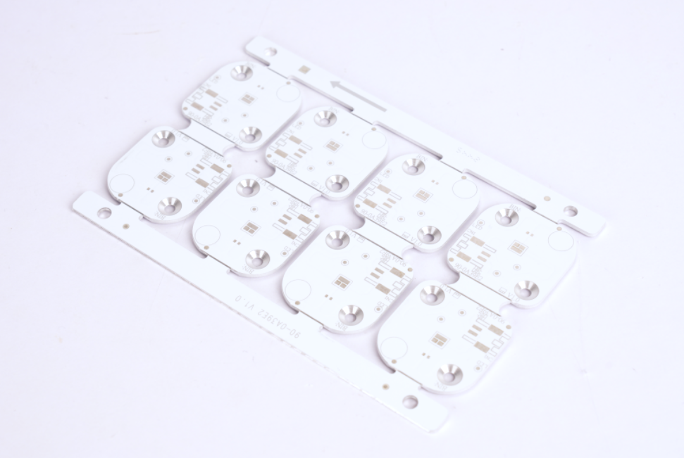
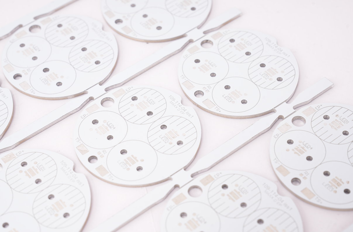
- High-Power LED Lighting (e.g., stage lights, grow lights).
- New Energy Vehicle Power Modules (motor controllers, on-board chargers).
- 5G Base Station RF Power Amplifier Units.
- Industrial Servo Drives.
- Medical Imaging Equipment Thermal Management Modules (CT machines, ultrasound probes).
- Aviation Electronics (airborne radars, satellite communication modules).
4 Layer Aluminum PCB Design Specification
| Design Parameter | Typical Value/Range |
| Aluminum Core Type | Thickness 1.0-3.0mm |
| Dielectric Layer Thermal Conductivity | ≥1.5W/mK |
| Layer Stack Sequence | Total Thickness 1.6±0.2mm |
| Copper Thickness Selection | Outer Layer: 1-3oz / Inner Layer: 0.5-2oz |
| Thermal Resistance Calculation | Rθ < 2.5℃/W |
| Thermal Via Design | Hole Diameter 0.3mm / Pitch 1.5mm |
| Insulation Voltage Withstand | ≥3kV(AC) |
| Characteristic Impedance Control | ±10% Tolerance |
| Mounting Hole Position | M3/M4 Standard Hole Size |
| Warpage Control | ≤0.5% of Board Thickness |
| Solder Mask Opening | Opening Size ≥ Component Pad + 0.2mm |
| Surface Finish | ENIG 0.05-0.1μm |
| Thermal Cycling Test | No Delamination/Cracking |
| Insulation Resistance | ≥100MΩ (500VDC) |
4 Layer Aluminum PCB Board Design Guide
A guide to 4 layer aluminum PCB design:
1. Aluminum Core Substrate Selection
- Material Selection Rationale: 6061-T6 aluminum alloy (thermal conductivity: 167 W/mK, tensile strength: 310 MPa) is ideal for high-power applications; 5052 alloy offers superior corrosion resistance for humid environments. Compliance with ASTM B209 ensures material integrity, validated via salt spray testing (ASTM B117) for corrosion resistance.
- Surface Treatment Parameters: Anodizing employs sulfuric acid electrolyte (150–200 g/L) at 15–20 V for 30–45 minutes. Oxide film thickness (15–20 μm) is verified by eddy-current thickness gauge (±2 μm precision). Boiling water sealing ensures insulation resistance ≥100 MΩ (500 VDC).
- Flatness Control Standard: Three-point measurement mandates ≤0.5% board thickness tolerance (e.g., ≤0.008 mm for 1.6 mm boards), validated by laser profilometry with traceable DFMEA documentation.
2. Thermal Dielectric Layer Design
- Material Performance Validation: Thermal conductivity ≥1.5 W/mK is confirmed via laser flash analysis (ASTM E1461). Recommended composite: epoxy resin with 60–70% volume fraction of 5–15 μm alumina filler. Glass transition temperature (Tg ≥150°C) and CTE (≤25 ppm/°C) are verified by DSC and TMA testing, respectively.
- Lamination Process Control: Vacuum hot-pressing at 180–200°C, 3–5 MPa for 90–120 minutes achieves thickness uniformity ≤±5% (X-ray thickness gauge). Adhesion strength ≥0.8 kN/cm is validated by microsection analysis per IPC-TM-650.
3. Stack-Up Optimization
- Symmetric Layer Design: “Aluminum base–dielectric–copper foil–PP sheet–inner layer–PP sheet–copper foil” symmetry ensures total thickness 1.6 ±0.2 mm. ANSYS thermal simulation confirms warpage ≤0.5% board thickness.
- Drilling Parameters: High-speed drilling uses 0.3 mm tungsten carbide bits at 50,000–60,000 rpm with 0.5–1.0 m/min feed rate. Hole wall roughness ≤25 μm is inspected optically; plasma desmear ensures cleanliness per IPC-6012.
4. Copper Thickness Allocation
- Current Density Calculation: Outer layer 1–3 oz (35–105 μm) follows J=I/(w×t) with ≤4 A/mm² current density. Inner layer 0.5–2 oz (17–70 μm) utilizes pulse plating for localized thickness enhancement.
- Trace Design Rules: Minimum trace/space meets manufacturing capability (e.g., 0.1 mm/0.1 mm). Etch factor ≥2.5 is verified by metallographic microscopy. Differential pair impedance is controlled within ±10% via Polar Si9000 calculations and TDR validation.
5. Thermal Management Solutions
- Thermal Via Arrays: 0.3 mm via diameter/1.5 mm pitch design is thermally validated by Rθ=ΔT/P. Electroplated copper filling achieves ≥95% fill rate, confirmed by cross-sectional analysis.
- 3D Thermal Simulation: ANSYS Icepak models power density ≤5 W/cm², ensuring critical components operate ≤125°C. Post-thermal cycling (-55°C~125°C, 1000 cycles) acoustic microscopy confirms no delamination/cracking.
6. Electrical Performance Assurance
- Dielectric Withstanding Voltage: ≥3 kV AC is ensured by dielectric thickness (≥0.1 mm) and material selection. Hipot testing (3 kV AC, 1 min) confirms no breakdown. Insulation resistance ≥100 MΩ (500 VDC) is validated by pressure cooking (85°C/85% RH, 168 h).
- Impedance Control: ±10% tolerance for characteristic impedance is achieved via differential pair design and TDR verification.
7. Mechanical Enhancement Strategies
- Warpage Mitigation: Symmetric stack-up and stress compensation limit warpage ≤0.5% board thickness. M3/M4 mounting holes feature ≥25 μm plated wall thickness (X-ray inspection).
- Solder Mask Design: Opening size ≥ component pad +0.2 mm is optically measured. LPI solder mask ensures edge smoothness ≤0.1 mm and 20–30 μm thickness (film thickness gauge).
8. Surface Finish Selection
- ENIG Parameters: 3–8 μm nickel (XRF) and 0.05–0.1 μm gold (SEM) layers withstand -40°C~125°C thermal shock (500 cycles) and solderability tests (288°C, 3×10 s).
- Alternative Finishes: OSP suits lead-free soldering (≥260°C tolerance); immersion silver offers high conductivity (≥2×10⁵ S/cm) for RF applications. Selection balances cost and performance.
9. Reliability Verification System
- Thermal Cycling Test: Post-1000-cycle (-55°C~125°C) inspection includes acoustic microscopy and electrical testing.
- Thermal Stress Test: Solder dip (288°C, 3×10 s) followed by microsection analysis (≥0.8 kN/cm adhesion) and dye penetration testing.
10. Manufacturing Process Control
- Drilling Accuracy: X-ray drilling achieves ±50 μm positional accuracy. AOI covers defect detection (shorts/opens, mask defects) per IPC-A-600.
- Lamination Monitoring: Real-time pressure (±5%) and temperature (±2°C) control via sensors. Microsection and dye testing data are logged in MES for traceability.
How to Make a 4 Layer Aluminum Printed Circuit Board?
4-Layer Aluminum PCB Manufacturing Process:
1. Material Preparation & Substrate Pretreatment
- Substrate Selection: Use 6061-T6/5052 aluminum alloy (thermal conductivity: 167/190 W/mK) with 1.0–3.0 mm thickness. Surface undergoes anodizing treatment (oxide film 15–20 μm) and salt spray testing (ASTM B117) for corrosion resistance. Copper foil thickness follows design specifications (outer layer: 1–3 oz; inner layer: 0.5–2 oz) with flatness ≤0.5% board thickness.
- Cutting & Cleaning: Precision cutting to design dimensions followed by ultrasonic cleaning to remove contaminants. Protective film applied to aluminum surface to prevent scratches; gloves mandatory during handling.
2. Inner Layer Core Board Fabrication
- Pattern Transfer: Clean copper-clad laminate, apply photoresist, and transfer circuit patterns via UV exposure (15–20 mJ/cm² energy). Develop and cure photoresist to form protective layer.
- Etching & Stripping: Alkaline etching (e.g., NaOH) removes unprotected copper; line width/spacing verified via metallographic microscopy (etch factor ≥2.5). Photoresist stripped post-etching; circuit integrity checked for opens/shorts.
3. Lamination Process
- Stack-Up Structure: Symmetric “aluminum base–dielectric–copper foil–inner layer–PP sheet” configuration ensures total thickness 1.6 ±0.2 mm. Dielectric layer uses high-thermal-conductivity epoxy resin with ceramic fillers (≥1.5 W/mK); pre-lamination vacuum baking removes moisture.
- Hot Pressing: Vacuum hot press at 180–200°C/3–5 MPa for 90–120 minutes ensures PP sheet fusion. Post-lamination X-ray inspection verifies layer alignment (≤±50 μm); warpage ≤0.5% board thickness via laser measurement.
4. Drilling & Hole Metallization
- Drilling Parameters: Tungsten carbide drill bits (0.3 mm diameter) operate at 50,000–60,000 rpm with 0.5–1.0 m/min feed rate. Plasma desmear cleans hole walls (IPC-6012 compliant).
- Copper Plating: Electroless copper + electroplating forms 25 μm copper layer. TDR testing validates impedance control (±10% tolerance); cross-section analysis confirms ≥95% fill rate.
5. Outer Layer Circuit Fabrication
- Pattern Transfer: Positive photoresist process for outer layers; alkaline etching forms circuits. Tin stripping retains protective layer. AOI inspects line width/spacing compliance.
- Surface Finish: ENIG (3–8 μm nickel/0.05–0.1 μm gold) verified by XRF/SEM. Alternatives include OSP (≥260°C heat resistance) or immersion silver (≥2×10⁵ S/cm conductivity) based on application requirements.
6. Solder Mask & Legend Printing
- Solder Mask Application: LPI solder mask applied via screen printing, pre-baked, exposed, and developed. Edge smoothness ≤0.1 mm; thickness 20–30 μm. Opening size ≥ component pad +0.2 mm ensures solderability.
- Legend Printing: Screen-printed component identifiers with clear, non-overlapping fonts. Cured for adhesion durability.
7. Profiling & Cutting
- V-Cut/Routing: V-Cut separates boards with burr height ≤25 μm. Precision routing ensures dimensional tolerance ≤±0.1 mm. Deburring performed post-cutting.
8. Testing & Inspection
- Electrical Testing: Flying probe tests verify connectivity; AOI detects shorts/opens; X-ray checks layer alignment. Insulation resistance ≥100 MΩ (500 VDC); dielectric strength ≥3 kV AC.
- Reliability Testing: Thermal cycling (-55°C~125°C, 1000 cycles), thermal shock (288°C solder dip ×3), and vibration testing per IPC-6012. Acoustic microscopy confirms no delamination/cracking.
9. Packaging & Shipment
- Cleaning & Packaging: Ultrasonic cleaning removes residues; vacuum packaging prevents moisture ingress. Packaging includes product labels and quality reports (dimensional, electrical, reliability data).
- Final Inspection: Full inspection by FQC and random checks by FQA ensure compliance with customer specifications and industry standards.
Why Choose Best Technology as 4 Layer Aluminum PCB Manufacturer?
Reasons why choose us as 4 layer aluminum PCB manufacturer:
- Cost Optimization Leadership: Leverage 19 years of process expertise and bulk procurement advantages to deliver cost-sensitive design solutions, reducing production costs by 15%-20% versus industry benchmarks while maintaining high performance.
- Certification Compliance: Full spectrum of certifications including ISO 9001, IATF 16949 (automotive), medical-grade approvals, and RoHS compliance, enabling seamless market access across automotive, medical, and consumer sectors.
- Free DFM Support: 19 years of aluminum PCB expertise identifies over 90% of early-stage manufacturability risks via free DFM analysis, reducing rework costs and time
- Reliable Delivery Performance: Achieve 99.2% on-time delivery rate through intelligent production scheduling and end-to-end visibility, minimizing supply chain risks and inventory pressure.
- Strict Quality Inspection: Implement 100% full-inspection with AOI/X-ray systems, achieving defect rates below 0.05% and exceeding industry standards for batch-to-batch consistency.
- Integrated One-Stop Service: Streamline design-prototype-production-testing workflows, cutting client coordination efforts by 40% and enhancing project efficiency from concept to mass production.
- Custom Technical Support: Provide specialized solutions for aluminum PCB thermal management and high-temperature reliability, including thermal simulation and impedance optimization.
- Rapid Response Excellence: Support 24-hour rapid prototyping for urgent orders, cutting development cycles by 50% compared to industry norms and accelerating market entry.
- Sustainable Manufacturing: Adopt eco-friendly processes and materials compliant with RoHS/REACH, supporting global market compliance and eco-certification goals.
Our Multilayer Aluminum PCB Capabilities
| Parameter | Capabilities |
| Base Material | Aluminum Base |
| Thermal Conductivity (Dielectric Layer) | 0.8 W/(m·K), 1.0 W/(m·K), 1.5 W/(m·K), 2.0 W/(m·K), 3.0 W/(m·K) |
| Board Thickness | 0.5mm~3.0mm (0.02″~0.12″) |
| Copper Thickness | 0.5 OZ, 1.0 OZ, 2.0 OZ, 3.0 OZ, up to 10 OZ |
| Outline Processing | Routing, Punching, V-Cut |
| Soldermask Color | White/Black/Blue/Green/Red Oil |
| Legend/Silkscreen Color | Black/White |
| Surface Finishing | Immersion Gold, HASL (Hot Air Solder Leveling), OSP (Organic Solderability Preservative) |
| Max Panel Size | 600mm × 500mm (23.62″ × 19.68″) |
| Packing Method | Vacuum Packaging/Plastic Bag Sealing |
| Sample Lead Time (L/T) | 4~6 Days |
| Mass Production Lead Time (MP) | 5~7 Days |
How to Get a Quote for Multilayer Aluminum PCB Project?
Multilayer Aluminum PCB Project Quote Request:
1. Board Specifications
- Layer Count: 4-layer (specified as aluminum-core).
- Dimensions: Exact PCB size (length × width × thickness).
- Material Type: Aluminum substrate (e.g., Al5052, Al6061) + FR4/epoxy dielectric layers.
- Surface Finish: ENIG, HASL, OSP, or other (specify for solderability/corrosion resistance).
2. Technical Parameters
- Minimum Trace Width/Spacing: Critical for manufacturing precision (e.g., 0.1mm/0.1mm).
- Impedance Control: Required tolerance (e.g., ±10% for RF/high-speed signals).
- Thermal Management Features: Thermal via density, heat sink integration, or copper pour requirements.
3. Production Details
- Order Quantity: Prototype (1-100pcs) / Small batch (100-1000pcs) / Mass production (1000+ pcs).
- Delivery Timeframe: Urgent (3-5 days) / Standard (7-10 days) / Economy (14+ days).
- Special Requirements: Buried/blind vias, edge plating, conformal coating, or RoHS/REACH compliance.
4. Design Files
- Gerber RS-274X files + Drill drawings.
- BOM (Bill of Materials) if applicable.
- 3D STEP models for mechanical fit validation (optional but recommended).
Welcome to submit your Gerber files to us for a quote now: sales@bestpcbs.com.
News
Berita Olahraga
News
Berita Terkini
Berita Terbaru
Berita Teknologi
Seputar Teknologi
Drama Korea
Resep Masakan
Pendidikan
Berita Terbaru
Berita Terbaru
Berita Terbaru
Comments are closed, but trackbacks and pingbacks are open.