A fine-line HDI PCB is used for compact electronics that require fine-pitch components, microvias, dense routing and stable signal performance. It helps reduce board size while improving circuit density and reliability. This guide covers key design rules, trace width and spacing, materials, stackup, SAP vs mSAP, manufacturing process, quality testing, cost factors and supplier selection.
Are you worried about these problems in fine-line HDI PCB projects?
- Design challenges: Fine line HDI PCB signal integrity challenges may appear when high-speed traces, fine-pitch BGA escape routing, microvias, impedance control, return paths and dense layer transitions are not planned correctly.
- Prototype challenges: Small-batch fine-line HDI PCB prototype projects may face delayed engineering approval, material mismatch, microvia reliability concerns, line/space yield risk and repeated DFM corrections before production.
- Assembly challenges: Dense BGA packages, via-in-pad structures, small solder mask openings and tight component spacing may increase solder wicking, bridging, voiding, warpage and inspection difficulty during PCB assembly.
As a 20+ years PCB manufacturer, EBest Circuit provides design review, prototype manufacturing and assembly support for global OEM projects, engineering teams and electronics brands.
- Design solution: We review stackup, impedance, BGA fanout, microvia placement, trace spacing, reference planes and DFM rules before production to reduce signal loss, crosstalk, impedance deviation and redesign risk.
- Prototype solution: We confirm materials, copper thickness, HDI build-up, laser microvia structure, via filling, surface finish and test requirements before fabrication to improve prototype accuracy and shorten approval cycles.
- Assembly solution: We check via-in-pad filling, solder mask registration, BGA pad design, stencil opening, panelization and SMT inspection requirements before assembly to reduce solder defects and improve batch consistency.
Welcome to contact us if you have any request for HDI PCB design, prototype, manufacturing or assembly: sales@bestpcbs.com.
What Is a Fine-Line HDI PCB?
A fine-line HDI PCB is a high-density interconnect PCB built with narrow trace width, tight spacing, microvias, blind vias, buried vias and thin dielectric layers. It is designed for compact electronics where ordinary multilayer PCB routing cannot provide enough space.
It works by replacing large through-hole routing with laser microvias and short interconnection paths. This structure allows fine-pitch ICs, BGA packages, RF modules and high-speed interfaces to be routed in a smaller area.
The key value is higher circuit density with shorter signal paths. For products such as smartphones, 5G modules, medical devices, IoT sensors and compact industrial electronics, this structure helps reduce board size while keeping electrical performance stable.
What Are Advantages and Disadvantages of Fine Line HDI PCB?
Advanced fine line HDI PCB improves routing density and product miniaturization, but it also raises manufacturing difficulty. The design should balance space, signal speed, reliability, cost and production yield before using advanced fine-line rules.
Main advantages include:
- Higher routing density for fine-pitch BGA, CSP and compact modules.
- Smaller PCB size without reducing circuit functions.
- Shorter signal paths for high-speed and RF circuits.
- Lower via stub risk because microvias replace long through-hole transitions.
- Better product integration for thin, lightweight and portable electronics.
Main limitations include:
- Higher cost due to laser drilling, fine-line imaging and sequential lamination.
- Stricter DFM rules for line width, spacing, annular ring and registration.
- Higher yield risk if copper balance, lamination and via filling are not controlled.
- Longer engineering review before prototype approval.
- Less rework margin during SMT assembly because of dense layout and small pads.
Where Are Fine-Line HDI PCBs Commonly Used?
Fine-line HDI PCBs are used in electronics that require small size, high component density, stable signal transmission and reliable assembly. These products often contain fine-pitch ICs, RF sections, high-speed interfaces, sensors or compact mechanical structures.
Common applications include:
- Smartphones, tablets and wearable electronics.
- 5G modules, RF boards and communication devices.
- Medical diagnostic devices, portable monitors and compact instruments.
- IoT modules, smart sensors and wireless tracking products.
- Automotive electronics, radar modules and control units.
- Industrial controllers, compact power modules and robotics boards.
- Flexible and rigid-flex projects for limited-space designs.
Fine-line HDI PCB applications in smartphones are especially common because smartphones use dense BGA chips, RF modules, camera modules, antennas, battery management circuits and high-speed data interfaces in a very limited internal space.
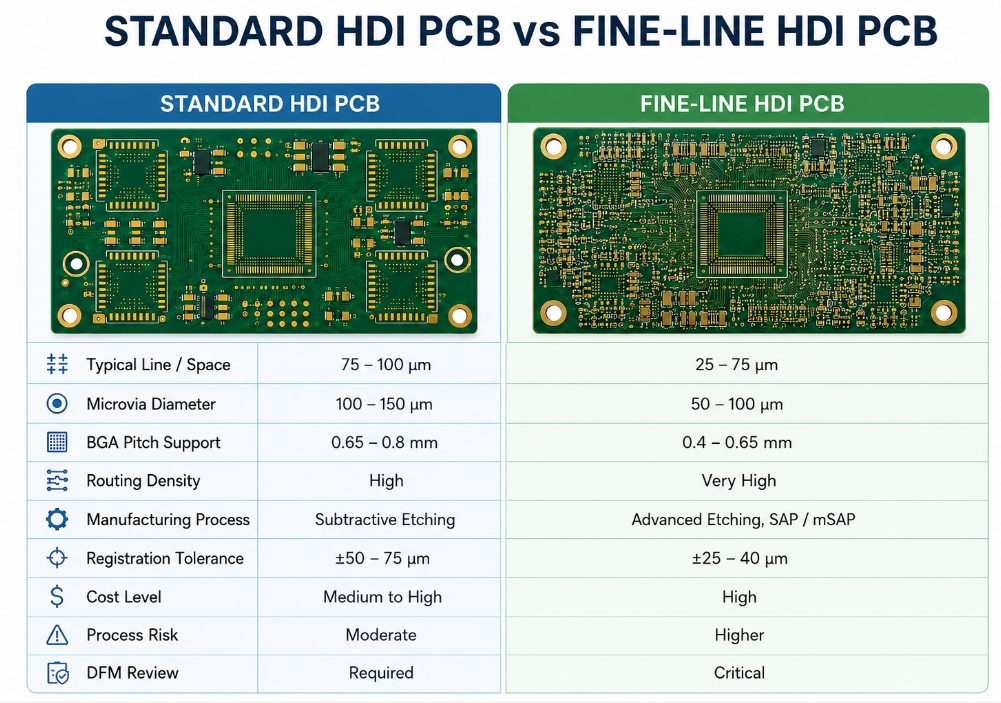
What Is the Difference Between Fine-Line and Standard HDI PCB?
A standard HDI PCB already uses microvias and higher routing density than a conventional multilayer PCB. A fine-line HDI PCB goes further by using narrower line/space, tighter registration, more precise imaging and more controlled plating.
| Item | Standard HDI PCB | Fine-Line HDI PCB |
|---|---|---|
| Typical line/space | 75–100 μm | 25–75 μm |
| Common process | Subtractive etching | Advanced etching, SAP or mSAP |
| Microvia size | 100–150 μm | 50–100 μm |
| BGA support | 0.65–0.8 mm pitch | 0.4–0.65 mm pitch |
| Routing density | High | Very high |
| Cost level | Medium to high | High |
| Process risk | Moderate | Higher |
| DFM review | Required | Critical |
The core difference is manufacturing tolerance. Fine-line structures leave less process margin, so stackup, copper thickness, line compensation, lamination and inspection should be confirmed before layout is finalized.
What Minimum Trace Width and Spacing Can Fine-Line HDI PCB Support?
Fine-line HDI PCB minimum trace width and spacing can commonly support 75/75 μm, 50/50 μm or 25/25 μm line and space, depending on copper thickness, process route, material, layer count and production volume. Smaller line/space does not always mean better design.
| Capability | Practical Range |
|---|---|
| Standard HDI line/space | 75/75 μm to 100/100 μm |
| Advanced fine line | 50/50 μm to 75/75 μm |
| Ultra fine line | 25/25 μm to 50/50 μm |
| Laser microvia diameter | 50–150 μm |
| Microvia aspect ratio | 0.75:1 preferred, 1:1 max |
| Controlled impedance tolerance | ±5% to ±10% |
| BGA pitch support | 0.4 mm to 0.8 mm |
| Finished copper | 12 μm to 35 μm typical |
The safest choice is not always the smallest trace. For better yield and cost control, use fine-line rules only in high-density areas such as BGA escape, and keep other routing areas wider when space allows.
What Technical Parameters Should Be Confirmed Before Fine-Line HDI PCB Design?
Before fine-line HDI PCB design, confirm line width, spacing, microvia size, dielectric thickness, copper weight, impedance, BGA pitch, surface finish and reliability class. These parameters affect routing density, yield, testability and price.
| Parameter | Recommended Check |
|---|---|
| Layer count | 4–16 layers based on routing density |
| HDI structure | 1+N+1, 2+N+2, stacked or staggered |
| Line/space | 25/25 μm to 100/100 μm |
| Microvia | 50–150 μm laser drilled |
| Via filling | Copper filling for via-in-pad or stacked vias |
| Copper weight | 0.5 oz to 1 oz for fine-line layers |
| Dielectric thickness | 50–100 μm common for build-up layers |
| Impedance | 50Ω single-ended, 90Ω or 100Ω differential |
| Surface finish | ENIG, ENEPIG, immersion silver or OSP |
| Standards | IPC-2226, IPC-6012, IPC-A-600, RoHS |
Early parameter confirmation prevents redesign. Once BGA fanout, stackup and impedance are fixed, late changes may affect the whole PCB layout, drill plan, lamination structure and assembly result.
What Substrate Materials Are Used in Fine-Line HDI PCB?
Fine line HDI PCB substrate materials should support laser drilling, stable lamination, low dielectric loss, dimensional stability and reliable copper adhesion. Material selection depends on signal speed, thermal stress, layer count and product environment.
Common substrate materials include:
- High-Tg FR-4: Suitable for many industrial, IoT and consumer products.
- Low-Dk/low-Df laminate: Better for high-speed, RF, 5G and low-loss signal transmission.
- Halogen-free laminate: Used when environmental compliance is required.
- BT resin or advanced build-up material: Used for fine pitch and very high-density structures.
- Flexible polyimide: Used in flexible fine-line HDI PCB and rigid-flex projects.
For high-speed designs, material loss matters as much as routing density. A low-Df laminate helps reduce insertion loss, while stable CTE helps reduce microvia cracking during reflow and thermal cycling.
How Should Fine-Line HDI PCB Stackup Be Designed?
A fine-line HDI PCB stackup should be designed around routing density, microvia structure, impedance control, power integrity, copper balance and assembly flatness. The stackup should be confirmed before PCB layout begins because BGA escape routing, dielectric thickness, drill pairs and impedance values are all connected.
A good stackup gives high-speed traces a stable reference plane, keeps microvias short, reduces via stubs and improves lamination reliability. For fine-pitch BGA, the most common HDI structures are 1+N+1 and 2+N+2, depending on routing density and layer count.
Example: 8-layer fine-line HDI PCB stackup for compact high-speed electronics
| Layer | Function | Design Notes |
|---|---|---|
| L1 | Component + signal | BGA escape, short high-speed routing, microvia to L2 |
| L2 | Ground plane | Continuous reference plane for L1 |
| L3 | Signal | Controlled impedance routing |
| L4 | Power plane | Main power distribution |
| L5 | Ground plane | Return path and shielding |
| L6 | Signal | High-speed or control signal routing |
| L7 | Ground or power plane | Reference plane for L8 |
| L8 | Component + signal | Bottom-side components and routing |
Key stackup rules:
- Use continuous ground planes near high-speed layers. This helps reduce impedance variation, crosstalk and EMI risk.
- Keep microvias short and manufacturable. Laser microvias are usually used between adjacent layers, such as L1-L2 or L8-L7.
- Avoid unnecessary stacked microvias. Stacked vias save space but increase plating and reliability risk.
- Use staggered microvias when possible. They are often easier to manufacture and more stable for thermal cycling.
- Balance copper on both sides. Uneven copper distribution may cause warpage during lamination, reflow or assembly.
- Confirm dielectric thickness early. Dielectric thickness directly affects impedance, trace width and routing rules.
- Separate noisy power areas from sensitive signals. RF, high-speed digital and analog sections should have clean return paths.
For most fine-line designs, the safest approach is to use fine-line rules only where routing density requires them. BGA escape areas may use 50/50 μm or smaller line/space, while less dense areas can use wider traces to improve yield and reduce cost.
Fine-Line HDI PCB Design Guidelines and Considerations
This design work should follow a clear engineering sequence. The goal is to prevent routing failure, signal integrity problems, microvia reliability issues and assembly defects before production starts.
Step 1: Confirm manufacturing capability before layout.
Before routing, confirm the manufacturer’s minimum line width, spacing, laser microvia size, copper thickness, via filling capability, solder mask registration and impedance tolerance. Do not rely only on CAD default rules.
Step 2: Define the BGA escape strategy.
For 0.4 mm, 0.5 mm or 0.65 mm pitch BGA packages, choose dog-bone fanout, via-in-pad, blind vias or microvias based on available routing channels. If via-in-pad is used, confirm copper filling and planarization before assembly.
Step 3: Build the stackup around signals and return paths.
High-speed traces should route over continuous ground planes. Avoid routing critical signals across split planes, voids or layer transitions without nearby ground stitching vias.
Step 4: Control impedance from the beginning.
Single-ended and differential impedance should be calculated before layout. Common targets include 50Ω single-ended, 90Ω differential and 100Ω differential, depending on the interface.
Step 5: Reduce fine-line routing only to critical areas.
Use the smallest line/space only in BGA breakout or dense routing zones. Wider routing in open areas improves manufacturing yield and cost control.
Step 6: Manage microvia reliability.
Keep laser microvias on adjacent layers when possible. Avoid deep microvias, excessive stacked vias and unsupported via structures. For stacked microvias, copper filling quality should be confirmed.
Step 7: Protect signal integrity.
Fine line HDI PCB signal integrity challenges often come from impedance mismatch, long parallel traces, poor return paths, dense via transitions and weak grounding. Keep high-speed traces short, matched and referenced to solid planes.
Step 8: Check solder mask and pad design.
Fine-pitch pads require accurate solder mask opening and registration. Poor solder mask control may cause solder bridging, insufficient solder or BGA assembly defects.
Step 9: Plan assembly before fabrication.
Via-in-pad, BGA pitch, stencil thickness, component spacing, panelization and inspection method should be reviewed before PCB manufacturing. Dense HDI boards leave little room for SMT rework.
Step 10: Run DFM review before prototype.
A DFM review should check line/space, annular ring, drill-to-copper clearance, copper balance, impedance coupon, solder mask clearance, surface finish and panel design. This step reduces engineering questions and prototype delays.
SAP vs mSAP in Fine-Line HDI PCB: Which Process Should You Choose?
SAP and mSAP are advanced processes used when traditional subtractive etching cannot hold very fine line and spacing with stable yield. For most fine-line HDI PCB projects, the decision depends on target line/space, copper thickness, routing density, cost target and production volume.
| Item | SAP | mSAP |
|---|---|---|
| Full Name | Semi-Additive Process | Modified Semi-Additive Process |
| Main Principle | Builds copper traces from a very thin seed layer | Uses a thin base copper layer and selective copper plating |
| Typical Line/Space | Below 25/25 μm in advanced applications | 25/25 μm to 50/50 μm commonly used |
| Best For | Ultra-fine substrate-like structures | Fine-line HDI PCB and compact electronic modules |
| Copper Control | Very precise | Precise and more practical for PCB production |
| Cost Level | Higher | Lower than SAP in many HDI projects |
| Production Difficulty | Very high | High but more widely used |
| Yield Risk | High if process control is weak | More stable for many fine-line HDI projects |
| Application | IC substrates, ultra-dense packaging, advanced modules | Smartphones, wearable devices, 5G modules, medical electronics |
| When to Choose | When ultra-fine line/space is required | When traditional etching cannot meet fine-line HDI routing needs |
Choose SAP when the design requires extremely fine traces close to substrate-level density. It is suitable for advanced miniaturized electronics where normal HDI PCB manufacturing cannot meet the routing requirement.
Choose mSAP when the project needs fine-line HDI PCB routing, high BGA density and better line control without moving to the highest-cost substrate process. It is often a practical choice for 25/25 μm to 50/50 μm line/space.
For many commercial fine-line projects, mSAP offers a better balance between density, manufacturability, cost and production stability. However, the final choice should be confirmed by line/space, copper thickness, layer structure and batch quantity.
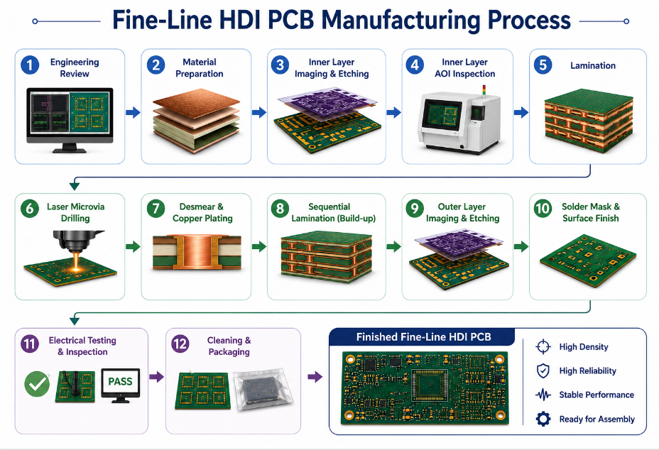
How Does the Fine-Line HDI PCB Manufacturing Process Work?
The fine-line HDI PCB manufacturing process requires tighter control than standard multilayer PCB production. Each step affects trace accuracy, microvia reliability, impedance and final assembly yield.
Step 1: Engineering review
The manufacturer reviews Gerber files, drill files, stackup, material, copper thickness, impedance requirement, line/space, BGA pitch, HDI structure and surface finish. This step confirms whether the design matches real production capability.
Step 2: Material preparation
The selected laminate, copper foil, prepreg and build-up materials are prepared according to the approved stackup. For high-speed products, low-Dk and low-Df materials may be used to reduce signal loss.
Step 3: Inner layer imaging and etching
The inner layers are coated, exposed, developed and etched. Fine-line imaging requires accurate pattern transfer and strict etching compensation to prevent line width loss, open circuits or copper residue.
Step 4: Inner layer inspection
AOI checks the inner layer pattern before lamination. This is important because inner layer defects cannot be repaired after the stackup is pressed together.
Step 5: Lamination
Core layers, prepreg and copper foil are laminated under controlled heat and pressure. Fine-line HDI PCB lamination must control resin flow, copper balance, dimensional stability and layer registration.
Step 6: Laser microvia drilling
Laser drilling forms microvias between adjacent layers. The process must control via diameter, depth, position accuracy and dielectric removal to ensure reliable plating.
Step 7: Desmear and copper plating
The drilled microvias are cleaned and prepared for metallization. Copper plating builds electrical connection through the vias. For via-in-pad and stacked microvias, copper filling may be required.
Step 8: Sequential lamination
For 1+N+1 or 2+N+2 HDI structures, laser drilling, plating and lamination may be repeated. More build-up layers increase routing density but also raise cost and process risk.
Step 9: Outer layer imaging and fine-line etching
The outer layers are imaged and etched with tight process control. If the design uses mSAP or SAP, selective copper build-up and flash etching are used to form finer traces.
Step 10: Solder mask and surface finish
Solder mask is applied to protect copper and define pads. Then surface finish such as ENIG, ENEPIG, OSP or immersion silver is applied based on assembly and reliability requirements.
Step 11: Electrical testing and final inspection
The boards go through E-test, AOI, impedance test, dimensional inspection and appearance check. For high-density designs, X-ray or cross-section checks may also be used.
Step 12: Packaging or assembly preparation
Finished boards are cleaned, packed and prepared for shipment or SMT assembly. If assembly is required, panelization, stencil design, BGA inspection and component placement files are reviewed before production.
What Quality Tests Are Required for Fine-Line HDI PCB Manufacturing?
Fine-line HDI PCB quality testing should focus on fine trace accuracy, microvia reliability, impedance stability, surface finish and assembly readiness. Because the line/space is very small, minor defects may cause open circuits, shorts, soldering defects or field failure.
- Material inspection
Check laminate, copper foil, prepreg, build-up material and material lot before production. Stable materials help control lamination, impedance and microvia reliability. - AOI inspection
AOI checks fine traces, spacing, copper residue, opens, shorts and pattern distortion. Inner layer AOI is especially important because hidden defects cannot be repaired after lamination. - Lamination inspection
Check board thickness, layer registration, resin flow, copper balance and warpage. Poor lamination may cause delamination, layer shift or microvia cracking. - Microvia inspection
Check laser microvia diameter, depth, position and cleanliness. Poor laser drilling may lead to plating voids, weak connections or reliability risks. - Plating and via filling inspection
Check copper plating thickness, via wall quality and filling condition. For via-in-pad and stacked microvias, poor filling may cause voids, solder wicking or BGA soldering defects. - Cross-section analysis
Cross-section checks copper thickness, microvia filling, via wall quality and interlayer connection. It is useful for high-reliability fine-line HDI PCB projects. - Electrical testing
100% E-test checks circuit continuity and insulation. It helps find tiny opens and shorts that may not be visible during appearance inspection. - Impedance testing
Controlled impedance coupons should be tested for high-speed designs. Common tolerance is ±5% to ±10%, depending on the project requirement. - X-ray inspection
X-ray checks hidden via filling, stacked microvia alignment and via-in-pad structures. It is useful for dense HDI designs with internal connection risks. - Solderability and surface finish inspection
Check ENIG, ENEPIG, OSP or immersion silver for thickness, oxidation, contamination and pad flatness. Good surface finish improves fine-pitch SMT assembly quality. - Warpage and final inspection
Check board flatness, dimensions, solder mask, silkscreen, cleanliness, quantity and packing before shipment. Flatness is especially important for BGA and thin HDI boards.
These tests help reduce open circuits, short circuits, microvia failure, impedance deviation, soldering defects and batch quality risks. For this manufacturing work, quality control should run through the whole process, not only the final inspection.
What Factors Affect Fine-Line HDI PCB Cost?
Cost is mainly affected by line/space, layer count, lamination cycles, microvia structure, material grade, via filling, impedance control, inspection level and delivery urgency. Board size alone does not decide price.
| Cost Factor | Cost Impact |
|---|---|
| Line/space below 75/75 μm | Higher imaging and yield cost |
| 2+N+2 or higher HDI | More lamination cycles |
| Stacked microvias | Higher drilling and filling cost |
| Via-in-pad copper filling | Higher plating and planarization cost |
| Low-Dk material | Higher laminate cost |
| ENEPIG finish | Higher surface finish cost |
| Controlled impedance | Coupon and test cost |
| Small batch prototype | Higher unit price |
| Urgent lead time | Higher production scheduling cost |
To control cost, avoid over-design. Use the finest line only in BGA escape or high-density zones, and keep other areas at wider rules when board space allows.
How to Choose Reliable Fine-Line HDI PCB Manufacturers?
Fine line HDI PCB manufacturers should provide more than fabrication. The supplier should help review the design, control advanced processes, test critical structures and support prototype-to-mass-production transition.
Key selection points include:
- Check real fine-line capability.
Ask for production-level line/space capability, not only laboratory capability. A manufacturer may claim 25/25 μm, but stable batch production may require different design rules. - Confirm HDI build-up experience.
The supplier should understand 1+N+1, 2+N+2, stacked microvias, staggered microvias, blind vias, buried vias and via-in-pad structures. - Review laser drilling control.
Laser microvia diameter, depth, taper, registration and cleanliness directly affect plating reliability. Poor microvia control may cause intermittent failure after thermal stress. - Check via filling and planarization ability.
For fine-pitch BGA, via-in-pad usually requires copper filling and flat pad surfaces. Poor filling may cause solder wicking, voids or weak BGA joints. - Ask for stackup and impedance support.
A reliable supplier should help check dielectric thickness, copper weight, material Dk/Df, impedance calculation and reference plane structure before production. - Confirm etching capability.
If the design uses 50/50 μm or smaller line/space, the manufacturer should explain the suitable mSAP route, HDI PCB fine line etching capability, copper thickness limit and expected yield. - Check inspection equipment.
AOI, E-test, X-ray, cross-section, impedance testing and solderability testing are important for fine-line HDI PCB quality control. - Evaluate DFM response speed.
Fine-line projects often require engineering questions before production. Slow feedback may delay prototype approval and affect product launch. - Review assembly experience.
If the project includes PCBA, the manufacturer should understand BGA assembly, stencil design, via-in-pad, solder mask registration, warpage control and functional testing. - Confirm standards and compliance.
Ask whether the supplier can support IPC standards, UL, RoHS, customer quality reports and export documentation according to project needs. - Check prototype and mass production consistency.
The process used for prototype should be scalable to mass production. Otherwise, the first batch may pass while later batches face yield or cost problems. - Avoid choosing only by low price.
Fine-line board failures can cause redesign, delivery delay, assembly scrap and field return. A slightly lower quote may cost more if process control is weak.
The best manufacturer should provide clear engineering feedback before production, not only accept files and quote quickly. For advanced fine-line designs, early technical communication is one of the strongest indicators of supplier reliability.
Why Choose EBest for Fine-Line HDI PCB Manufacturing?
EBest Circuit provides design review, prototype, mass production, component sourcing and PCB assembly support. For customers, this helps reduce communication cost, engineering errors and production delay.
- One-stop PCB and PCBA service
EBest supports PCB design, prototype, mass production, component sourcing and assembly. Customers can manage the project through one supplier instead of coordinating several vendors. - 20+ years of manufacturing experience
Founded in 2006, EBest has long-term experience in custom PCB manufacturing. This helps customers identify stackup risks, line/space limits, microvia issues and assembly concerns before production. - Prototype to mass production support
EBest can support small-batch prototypes and batch production. Customers can verify the design first, improve DFM details and then move to volume manufacturing with a more stable process. - Wide PCB manufacturing capability
EBest manufactures HDI PCB, multilayer PCB, FR4 PCB, high frequency PCB, high speed PCB, impedance control PCB, flexible PCB, rigid-flex PCB, ceramic PCB, metal core PCB and heavy copper PCB. This is useful for projects involving HDI, RF, high-speed or thermal requirements. - Fine-line HDI engineering review
Fine-line designs often involve dense BGA routing, narrow trace spacing, laser microvias, via-in-pad and impedance control. EBest reviews these details before production to reduce redesign and prototype failure risk. - Stable production capacity
EBest has a monthly capability of 260,000 square feet, around 28,900 square meters. This helps customers handle prototype orders, repeat orders and growing production demand. - Quick-turn support for urgent projects
For urgent boards, EBest can provide expedited service, and qualified urgent projects can be shipped within 24 hours. This helps engineering teams shorten validation and testing cycles. - Certified quality system
EBest holds ISO 9001:2015, IATF 16949, ISO 13485:2016, AS9100D, UL, RoHS and REACH certifications. These certifications support customers in automotive, medical, aerospace, industrial and export projects. - Support for high-speed and impedance control designs
This board type is often used in compact high-speed products. EBest helps review signal layers, reference planes, dielectric thickness and impedance targets before manufacturing. - Assembly support for dense layouts
EBest reviews BGA pads, via-in-pad filling, solder mask registration, stencil openings and component spacing before assembly. This helps reduce solder bridging, solder wicking, voiding and rework risk. - China source factory with global supply
EBest provides custom PCB and PCBA solutions for global OEM and ODM customers. Customers can use EBest for prototype, manufacturing and assembly without relying on multiple middle suppliers.
FAQs About Fine Line HDI PCB
Q1: When should I use a fine-line HDI PCB instead of a standard PCB?
A1: Use this board type when the design has fine-pitch BGA, limited board space, high signal density or strict size requirements. If a standard multilayer PCB cannot route all signals without increasing board size, microvias and narrow line/space can help improve routing density.
Q2: Is fine-line HDI PCB suitable for 0.4 mm BGA packages?
A2: Yes. This board type is commonly used for 0.4 mm BGA and compact IC packages. These designs often require laser microvias, via-in-pad, tight solder mask registration and controlled pad flatness. The stackup and fanout method should be confirmed before PCB layout starts.
Q3: What is the common line width and spacing for fine-line HDI PCB?
A3: Common line/space includes 75/75 μm, 50/50 μm and 25/25 μm. The final value depends on copper thickness, layer count, material, process route and production quantity. For better yield, use the finest line only in dense routing areas.
Q4: Does fine-line HDI PCB always require mSAP or SAP?
A4: Not always. If the design uses 75/75 μm or similar rules, advanced subtractive etching may be enough. If the design requires 50/50 μm or below, mSAP may be more suitable. SAP is usually used for extremely fine substrate-like structures.
Q5: Why does fine-line HDI PCB cost more than standard HDI PCB?
A5: The cost is higher because this board requires tighter imaging, laser drilling, microvia plating, via filling, sequential lamination and more inspection steps. Cost also increases when the design uses stacked microvias, low-loss materials, controlled impedance or urgent prototype delivery.
Q6: What materials are commonly used for fine-line HDI PCB?
A6: Common materials include high-Tg FR-4, low-Dk/low-Df laminate, halogen-free laminate, BT resin and flexible polyimide. High-speed, RF and 5G products usually use low-loss materials. Flexible fine-line HDI PCB or rigid-flex structures may use polyimide-based materials.
Q7: Can fine-line HDI PCB be used for high-speed signals?
A7: Yes. This board can support high-speed signals when impedance, reference planes, return paths and via transitions are properly controlled. For DDR, USB, PCIe, RF or sensor interfaces, the design should avoid split planes, long stubs and uncontrolled layer transitions.
Q8: What causes signal integrity problems in fine-line HDI PCB?
A8: Signal integrity problems often come from impedance mismatch, poor return paths, long parallel routing, excessive via transitions, weak grounding or unsuitable materials. These risks increase in dense BGA areas, so stackup, dielectric thickness and routing rules should be reviewed before production.
Q9: Is via-in-pad necessary for fine-line HDI PCB?
A9: Via-in-pad is not always necessary, but it is often used for 0.4–0.65 mm BGA and compact layouts. It helps save routing space, but the via should be filled and planarized to prevent solder wicking, voids and poor BGA solder joints.
Q10: What tests are important for fine-line HDI PCB quality control?
A10: Important tests include AOI, E-test, X-ray, cross-section, impedance testing, solderability testing and final inspection. For this board type, microvia plating, via filling, line/space accuracy and impedance stability should be checked carefully before shipment or assembly.
Q11: What files should I prepare for fine-line HDI PCB quotation?
A11: Prepare Gerber files, drill files, stackup, material request, copper thickness, impedance requirements, surface finish, solder mask color, quantity, IPC class and delivery target. If assembly is required, also provide BOM, pick-and-place file and assembly drawings.
Q12: How can I reduce the cost of a fine-line HDI PCB project?
A12: Use fine-line rules only where routing density requires them, avoid unnecessary stacked microvias, choose practical materials and confirm the stackup early. Wider traces in open areas, simpler HDI build-up and clear DFM files can help reduce cost and improve production yield.
Q13: What should be checked before fine-line HDI PCB assembly?
A13: Before assembly, check BGA pad design, via-in-pad filling, solder mask opening, board flatness, surface finish, stencil thickness, panelization and component spacing. These checks help reduce solder bridging, solder wicking, BGA voiding, tombstoning and rework risk.
Q14: How do I choose a reliable fine-line HDI PCB manufacturer?
A14: Check real line/space capability, HDI build-up experience, laser drilling control, via filling quality, impedance testing, inspection equipment and assembly support. A reliable manufacturer should provide DFM feedback before production instead of only quoting from files.
Q15: Can EBest support fine-line HDI PCB prototype and assembly together?
A15: Yes. EBest Circuit supports fine-line HDI PCB design review, prototype, mass production, component sourcing and PCB assembly. This helps customers manage engineering review, bare board fabrication, component preparation and SMT assembly through one supplier.
Final Summary
This PCB structure is suitable for compact products with fine-pitch BGA, microvias, narrow trace spacing and high-speed signals. Before production, engineers should confirm stackup, material, impedance, microvia structure, surface finish and assembly requirements.
For buyers, a reliable supplier should provide DFM review, prototype support, stable manufacturing, quality testing and assembly coordination. This helps reduce redesign, delivery delay, soldering defects and batch quality risks.
EBest Circuit provides fine-line HDI PCB design review, prototype, mass production, component sourcing and PCB assembly. Send your files to EBest for a practical quotation: sales@bestpcbs.com.
Tags: Fine line HDI PCB manufacturers, Fine-Line HDI PCB Design Guidelines, Fine-line HDI PCB manufacturing process
PakarPBN
A Private Blog Network (PBN) is a collection of websites that are controlled by a single individual or organization and used primarily to build backlinks to a “money site” in order to influence its ranking in search engines such as Google. The core idea behind a PBN is based on the importance of backlinks in Google’s ranking algorithm. Since Google views backlinks as signals of authority and trust, some website owners attempt to artificially create these signals through a controlled network of sites.
In a typical PBN setup, the owner acquires expired or aged domains that already have existing authority, backlinks, and history. These domains are rebuilt with new content and hosted separately, often using different IP addresses, hosting providers, themes, and ownership details to make them appear unrelated. Within the content published on these sites, links are strategically placed that point to the main website the owner wants to rank higher. By doing this, the owner attempts to pass link equity (also known as “link juice”) from the PBN sites to the target website.
The purpose of a PBN is to give the impression that the target website is naturally earning links from multiple independent sources. If done effectively, this can temporarily improve keyword rankings, increase organic visibility, and drive more traffic from search results.
Comments are closed, but trackbacks and pingbacks are open.