How to design A FPGA PCB?â Discover its specification, benefits, application, and design guideline for FPGA PCB.
- Can BGA welding withstand high temperature aging?
- Why is my high-speed signal running slower and slower?
- Will multiple power supplies fight with each other?
Best Technology Can Provide You:
- Welding perspective: Each board is X-rayed, and solder joint defects are nowhere to be hidden.
- Signal highway: From drawing board to assembly, the signal is fully escorted.
- Power traffic light: Intelligently adjust the power-on timing to prevent power supply chaos.
Welcome to contact us if you have any request for FPGA PCBA service: sales@bestpcbs.com.
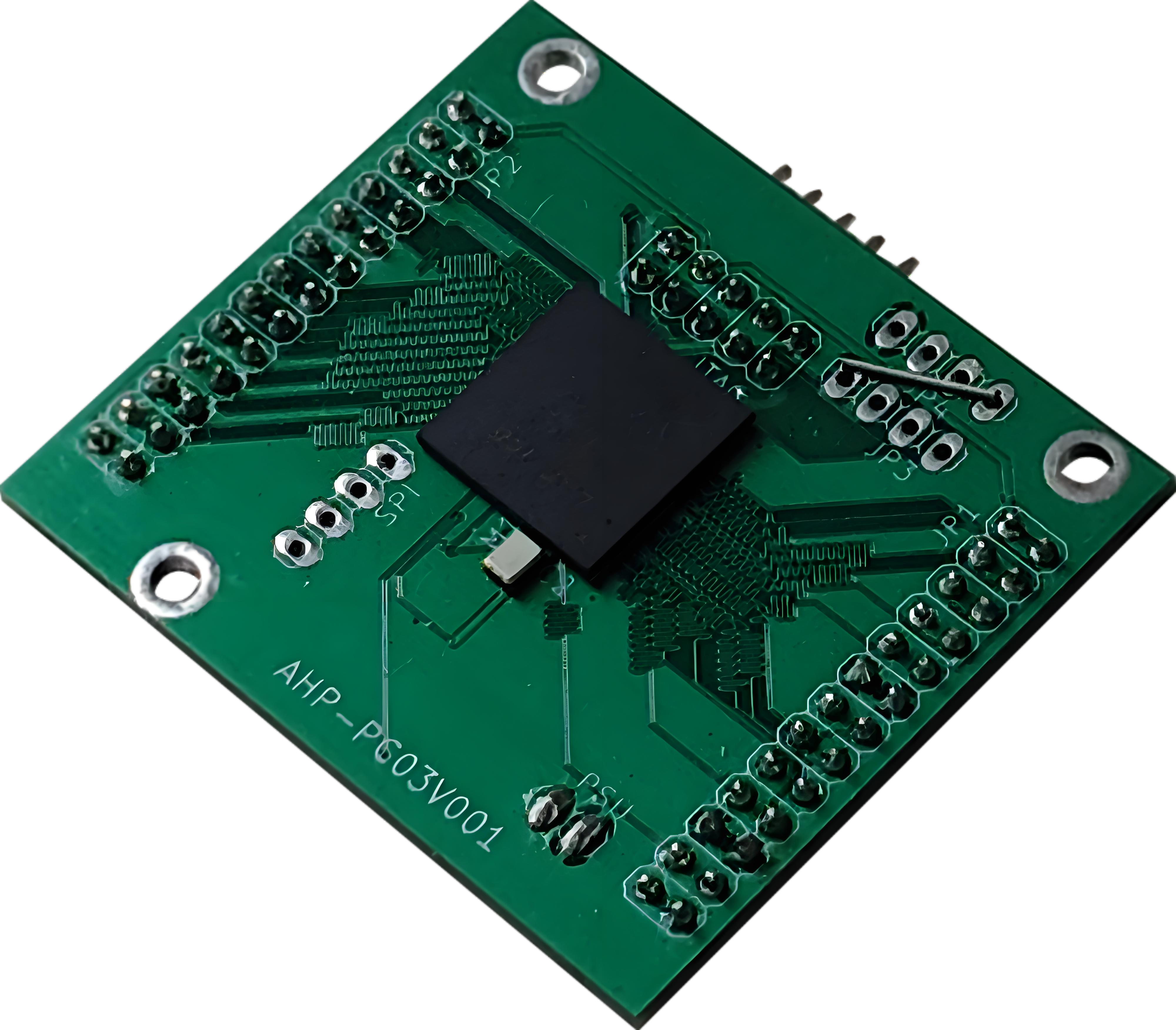
What Is FPGA PCB?
A FPGA PCB is a specially engineered printed circuit board that physically mounts and electrically integrates a field-programmable gate array semiconductor device with supporting hardware components, such as power regulators, memory units, clock sources, and input/output connectors.
This substrate features precisely routed copper traces to establish reliable electrical pathways, incorporating design elements for signal integrity in high-speed interfaces, stable multi-voltage power delivery, and efficient thermal dissipation to manage operational heat.
Once assembled, the board serves as a reconfigurable platform capable of implementing custom digital logic functions through post-manufacturing programming of the FPGA, enabling versatile applications like real-time data processing or communication bridging.
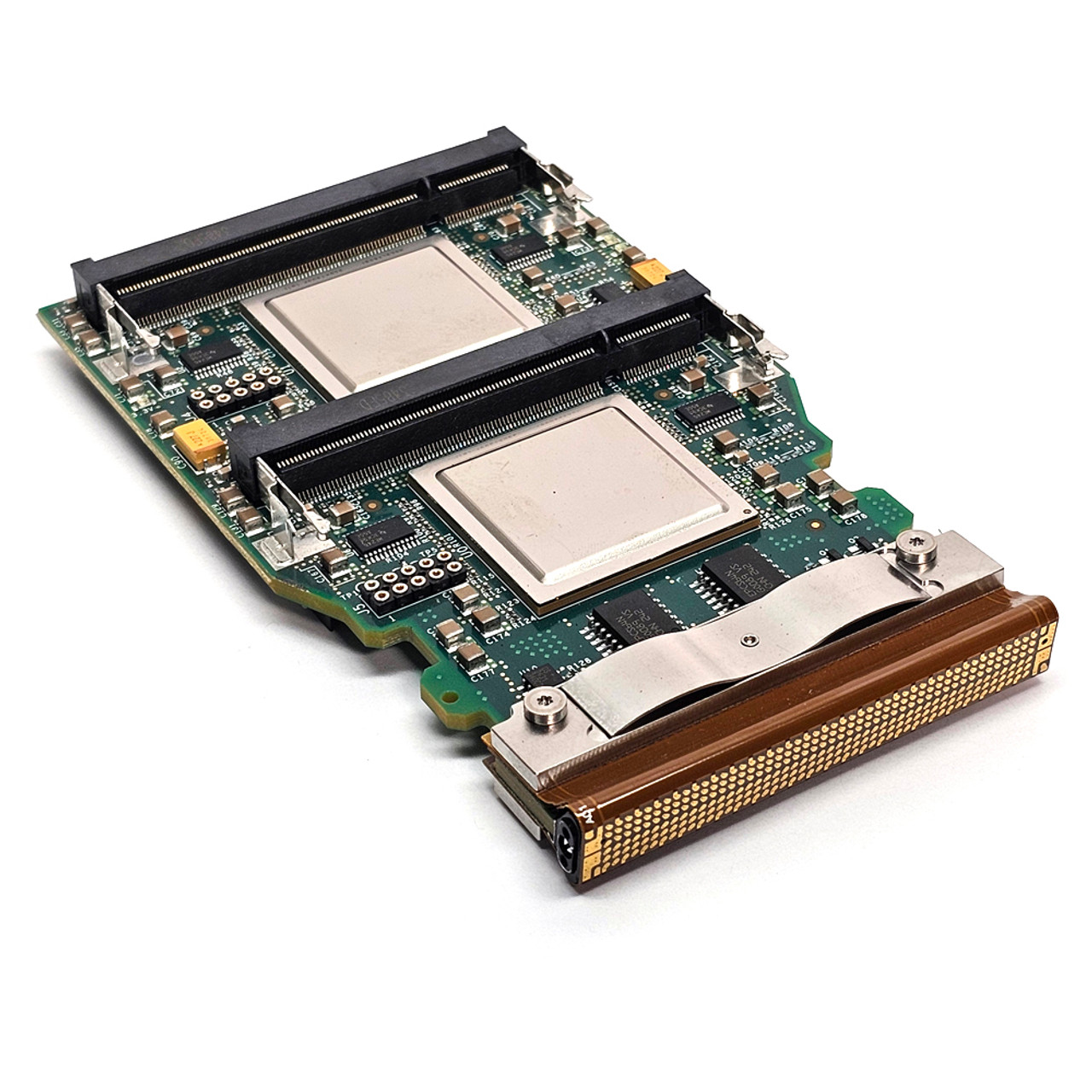
Components of FPGA PCB
1. Central Processing Unit
- Programmable logic blocks (CLBs, DSP slices).
- Configuration memory cells.
- Clock management circuits (PLLs/DCMs).
2. Power Delivery Network
- Multi-voltage regulators (1.0V core, 2.5V/3.3V I/O).
- Decoupling capacitors (0.1μF ceramic arrays).
- Power sequencing controllers.
3. Memory Subsystem
- Volatile storage (DDR3/DDR4 controllers).
- Non-volatile configuration memory (NOR Flash).
- Cache memory blocks.
4. Signal Interface Units
- High-speed serial transceivers.
- General-purpose I/O banks.
- Differential pair routing channels.
5. Support Circuits
- JTAG programming interface.
- Thermal monitoring sensors.
- Reset generation circuitry.
6. Mechanical Features
- Ball grid array (BGA) footprint
- Thermal relief patterns
- Board stiffeners (for large packages)
Why Use FPGA PCB?
- Flexible Hardware Reconfiguration: FPGAs enable post-production logic updates, allowing adaptive designs without physical hardware changes.
- Parallel Processing Capability: Customizable logic blocks execute multiple operations simultaneously, ideal for real-time signal processing.
- Low Latency for Time-Sensitive Tasks: Hardware-level processing achieves nanosecond response times, critical for industrial control systems.
- Energy Efficiency in Specialized Workloads: Dedicated circuits reduce power waste compared to general-purpose processors.
- Legacy System Modernization: Bridges outdated protocols with modern standards, extending equipment lifespan.
- Security Through Hardware Customization: Unique circuit layouts resist standardized attacks, enhancing tamper resistance.
- Rapid Iteration During Development: Immediate testing accelerates debugging versus semiconductor fabrication delays.
What Are Applications of FPGA PCB?
- Telecommunications – 5G baseband processing; Optical network conversion.
- Industrial Automation – Robotic arm control; Predictive maintenance systems.
- Medical Technology – Medical imaging acceleration; Portable diagnostic devices.
- Financial Technology – Low-latency trading systems; Real-time risk analysis.
- Aerospace & Defense – Satellite data processing; Radar systems.
- Automotive – Autonomous vehicle sensors; Vehicle network gateways.
- Consumer Electronics – Video transcoding; VR motion tracking.
- Energy Systems – Smart grid monitoring; Solar power optimization.
- Scientific Research – Physics experiments; Genomic sequencing
- IoT Infrastructure – Edge computing nodes; LPWAN base stations.
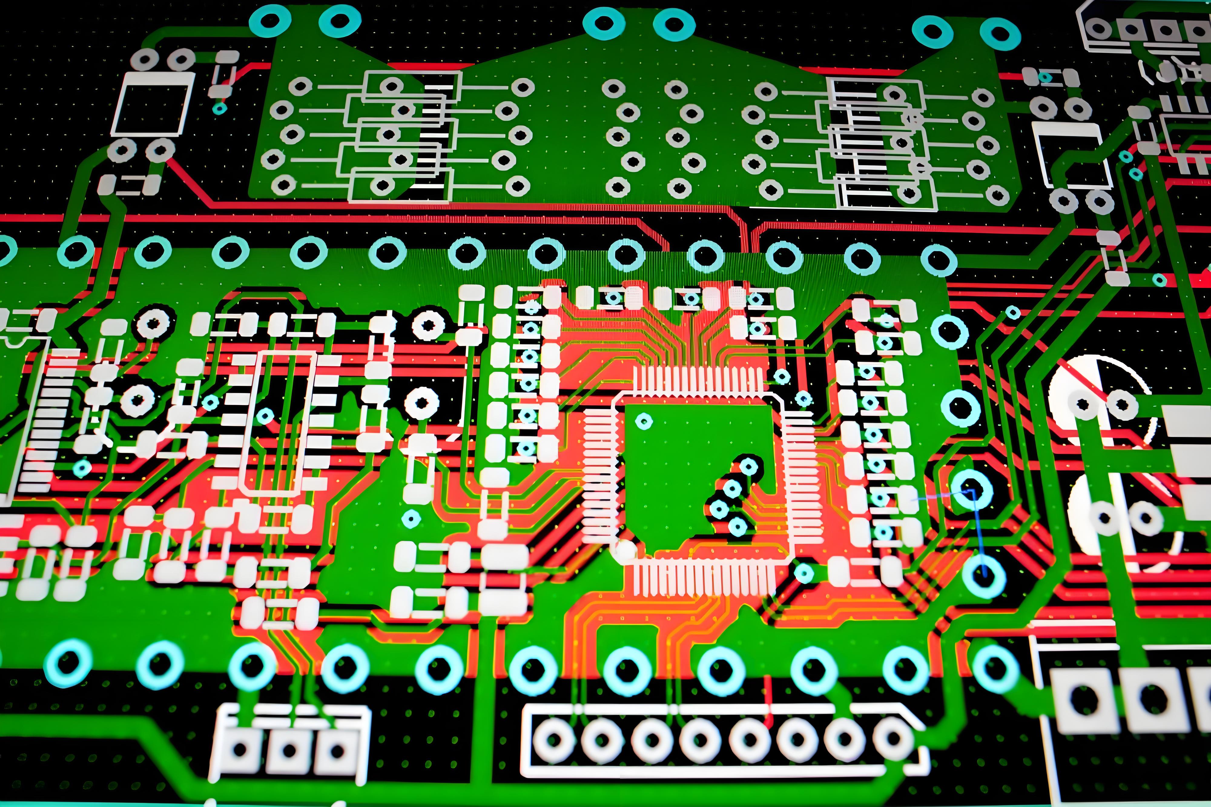
FPGA PCB Design Guidelines
Below are FPGA PCB design guidelines:
1. Layer Stack Management
- Use symmetrical stackup with adjacent power-ground plane pairs.
- Assign dedicated layers for high-speed signals with reference planes.
2. Power Delivery System
- Implement separate power islands for core, I/O and auxiliary voltages.
- Place decoupling capacitors in descending values (10μF to 100nF) near power pins.
3. Signal Routing Principles
- Maintain consistent impedance for differential pairs (+/- 10% tolerance).
- Route clock signals first with maximum ground shielding.
4. Thermal Considerations
- Use thermal vias under high-power components.
- Implement copper balancing for even heat distribution.
5. Manufacturing Compliance
- Follow 3W spacing rule for high-speed traces.
- Verify BGA escape routing meets fabrication capabilities.
6. Grounding Strategy
- Maintain continuous ground planes beneath sensitive circuits.
- Implement star grounding for mixed-signal systems.
7. Design Verification
- Perform post-layout SI/PI simulations.
- Validate timing margins with board-level models.
FPGA PCB Assembly Service â Best Technology
- Full Turnkey Solutionsâ â From PCB fabrication to final assembly and testing.
- âHigh-Mix, Low-Volume Expertiseâ â Optimized for FPGA prototyping & small-batch production.
- âDFM Optimizationâ â Early design feedback to minimize re-spins.
- âFlexible Packagingâ â Support for advanced ICs (BGA, QFN, 01005).
- Free DFM (Design for Manufacturability) Analysis: Optimizes PCB layouts to reduce material waste, lower production costs, and avoid late-stage design revisions.
- Turnkey Solutions â Full-service PCB manufacturing from design to delivery, accelerating your productâs time-to-market.
- Superior Quality â 100% inspection on bulk orders, ensuring reliability and consistency.
- Fast Turnaround â 24-hour rapid prototyping and industry-leading production lead times.
- Stable Supply Chain â Guaranteed material availability with minimal risk of delays.
- Competitive & Transparent Pricing â No hidden costs, offering the best value without compromising quality.
Our PCBA Capabilities
| Item | Capabilities |
| Placer Speed | 13,200,000 chips/day |
| Bare Board Size | 0.2 x 0.2 inches – 20 x 20 inches/ 22*47.5 inches |
| Minimum SMD Component | 01005 |
| Minimum BGA Pitch | 0.25mm |
| Maximum Components | 50*150mm |
| Assembly Type | SMT, THT, Mixed assembly |
| Component Package | Reels, Cut Tape, Tube, Tray, Loose Parts |
| Lead Time | 1 – 5 days |
FAQs
Q1: Why does my FPGA PCB fail to boot consistently after assembly?
A1: Check solder joint integrity â BGA voids exceeding 25% cause intermittent connections. Use X-ray inspection to verify void percentage. Ensure power sequencing matches FPGA datasheet requirements (typically core voltage before I/O banks).
Q2: How to resolve signal integrity issues in 10Gbps+ transceiver channels?
A2: Route differential pairs with <5mil length mismatch and insert ground-stitching vias every 150mil near SerDes lanes. Simulate with IBIS-AMI models to validate eye diagram margins pre-production.
Q3: Why do we encounter timing closure failures despite meeting constraints?
A3: Clock skew often originates from unequal via counts in global clock trees. Balance H-tree routing with matched via transitions (typically 8 vias per branch). Add programmable delay buffers for ±50ps fine-tuning.
Q4: What causes thermal runaway in high-density FPGA designs?
A4: Inadequate copper thickness in power planes (recommend 2oz for >15A currents). Implement thermal relief patterns under BGA with 0.3mm diameter voids. Monitor junction temperature using on-die sensors via I2C.
Q5: How to mitigate EMI from high-speed memory interfaces?
A5: Apply Ï-type EMI filters to DDR4 DQ lines (22Ω resistors + 100pF caps). Stagger memory chip placement to break resonant cavity effects. Use shielded flex cables for off-board connections exceeding 3Gbps.
Tags: FPGA PCB, FPGA PCB Design
You can leave a response, or trackback from your own site.
News
Berita Olahraga
News
Berita Terkini
Berita Terbaru
Berita Teknologi
Seputar Teknologi
Drama Korea
Resep Masakan
Pendidikan
Berita Terbaru
Berita Terbaru
Berita Terbaru
Comments are closed, but trackbacks and pingbacks are open.